
First SPIDAR chips take shape in the cleanroom
Work in SPIDAR’s fabrication work package is in full swing. Following the arrival of our first GaAs epitaxial wafers earlier this year, the team has been developing the core fabrication processes for our photonic integrated circuits (PICs) in the Micronova cleanroom at Aalto University.
Process development is the unglamorous but essential foundation of any new photonic platform: establishing reliable etch processes, lithography, contact metallization, and the other steps that every future SPIDAR device will depend on. The first complete devices, Fabry-Perot lasers that will serve as the platform’s baseline light sources, are the next step on the roadmap and we anticipate seeing “first light” soon.
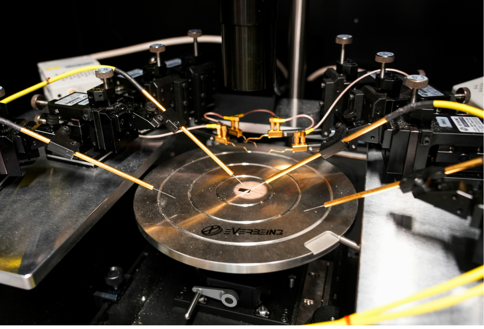
In parallel, the measurement setups for characterizing these first devices are taking shape in our testing lab, with the probe station for testing electrical contacts pictured above.